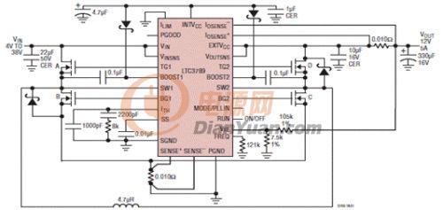
這個(gè)IC的設(shè)計(jì)難點(diǎn)在PCB,可能大多數(shù)的人都沒(méi)去仔細(xì)看DATASHEET, 另外因?yàn)椴季€復(fù)雜,建議用4層板。仔細(xì)看下下面的指導(dǎo)。如果需要技術(shù)支持,凌特的FAE愿意為您效勞 Q47401838
Use planes for VIN and VOUT to maintain good voltage
filtering and to keep power losses low.
? Flood all unused areas on all layers with copper. Flooding
with copper will reduce the temperature rise of power
components. Connect the copper areas to any DC
net (VIN or GND). When laying out the printed circuit
board, the following checklist should be used to ensure
proper operation of the LTC3789. These items are also
illustrated in Figure 13.
? Segregate the signal and power grounds. All smallsignal
components should return to the SGND pin at
one point, which is then tied to the PGND pin close to
the inductor current sense resistor RSENSE.
? Place switch B and switch C as close to the controller
as possible, keeping the PGND, BG and SW traces
short.
? Keep the high dV/dT SW1, SW2, BOOST1, BOOST2,
TG1 and TG2 nodes away from sensitive small-signal
nodes.
? The path formed by switch A, switch B, D1 and the CIN
capacitor should have short leads and PC trace lengths.
The path formed by switch C, switch D, D2 and the
COUT capacitor also should have short leads and PC
trace lengths.
? The output capacitor (–) terminals should be connected
as closely as possible to the (–) terminals of the input
capacitor.
? Connect the top driver boost capacitor CA closely to the
BOOST1 and SW1 pins. Connect the top driver boost
capacitor CB closely to the BOOST2 and SW2 pins.
? Connect the input capacitors CIN and output capacitors
COUT closely to the power MOSFETs. These capacitors
carry the MOSFET AC current in the boost and buck
region.
? Connect VFB pin resistive dividers to the (+) terminals of
COUT and signal ground. A small VFB bypass capacitor
may be connected closely to the LTC3789 SGND pin.
The R2 connection should not be along the high current
or noise paths, such as the input capacitors.
? Route SENSE– and SENSE+ leads together with minimum
PC trace spacing. Avoid having sense lines pass
through noisy areas, such as switch nodes. The filter
capacitor between SENSE+ and SENSE– should be as
close as possible to the IC. Ensure accurate current
sensing with Kelvin connections at the SENSE resistor.
One layout example is shown in Figure 14.
? Connect the ITH pin compensation network closely to
the IC, between ITH and the signal ground pins. The
capacitor helps to filter the effects of PCB noise and
output voltage ripple voltage from the compensation
loop.
? Connect the INTVCC bypass capacitor, CVCC, closely
to the IC, between the INTVCC and the power ground
pins. This capacitor carries the MOSFET drivers’ current
peaks. An additional 1μF ceramic capacitor placed immediately
next to the INTVCC and PGND pins can help
improve noise performance substantially.
APPLICATIONS INFORMATION
GND
VOUT